


Description
- Origin: Mainland China
- Output: Analog Sensor
- Theory: Optical Sensor
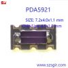
- Model Number: PDA5921
- Type: Optical-Electronics Sensor
- is_customized: Yes
- Material: Mixture
- Usage: Position Sensor
- Range of Spectral Bandwidth: 450—1100 nm
- Wavelength of Peak Sensitivity: 880 nm
- Open-Circuit Voltage: 0.4 V
- Reverse photosensitive current: 25 μA
- Dark Current: <50 nA
- Reverse Breakdown Voltage: >30 V
- Total Capacitance: 20 pF
- Rise/Fall Time: 30/30 nS
English is the original language, other languages are automatically translated, there may be translation errors
Can be customized according to customer requirements, please read the customization instructions at the bottom
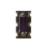
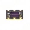
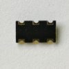
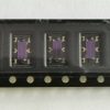
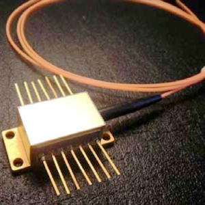
Photodiode Array, PDA5921
Optoelectronic detection sensor
COB package,bare chip
Chip size: 1.00mm x 4.50mm (0.039" x 0.177"), per elements
Range of Spectral Bandwidth: 450—1100nm
Wavelength of Peak Sensitivity: 880 nm
Open-Circuit Voltage: 0.4 V
Reverse photosensitive current: 25 uA
Dark Current: <50 nA
Reverse Breakdown Voltage: >30 V
Total Capacitance: 20 pF
Rise/Fall Time: 30/30 nS
For detailed product parameters, please check the specifications and download the specifications from the company's website
Factory direct sales, batch purchase customers can contact the seller to arrange production

Smilar product:
PDA5925 : Chip size 1.09mm*1.09mm,The positive and negative electrodes of the four diodes are independent.
PDA5926 : Chip size 2.04mm*2.04mm,The positive and negative electrodes of the four diodes are independent.
PDA5927 : Chip size 2.50mm*2.50mm,Four diodes with common cathode.
PDA5928 : Chip size 1.60mm*1.60mm,The positive and negative electrodes of the four diodes are independent.
One groups of balanced photodiodes:
PDA5921: Chip size 1.0mm*4.5mm
Two groups of balanced photodiodes:
PDA5922: Chip size 1.0mm*4.5mm
Can help customers develop similar products.
Since the similar products required by customers may be different, such as different PCB sizes, different PCB positioning holes, different chip positions, different chip sizes, different pad positions, etc., customers can provide detailed requirements, and our company can customize products according to customer requirements. Product prices may vary upon request. Please contact us if you need it.
Customization Instructions (Class A):
Class A design means that the customer provides the requirements, our company designs and produces, the customer does not need to bear the development cost, the customer only needs to purchase a certain number of products, and the copyright belongs to our company after the design is completed, and our company has the right to sell it publicly
1. Provide detailed PCB size requirements, including the location and size of PCB positioning holes.
2. Provide detailed requirements for chip size, including chip placement.
3. Provide other detailed requirements.
4. Assess Feasibility
5. Reply to the customer, if the evaluation is not feasible, reject; if feasible, will provide quotation and delivery time, communicate other problems.
6. Our company design PCB diagram.
7. Provide PCB design pictures and size pictures to customers for confirmation.
8. Customers pay for custom products
9. Our company produces products and ships them to customers.
Customization Instructions (Class B):
Class B design means that the customer provides the requirements, our company designs and produces, or the customer designs and produces by our company, and the customer needs to pay about 500 US dollars. After the design is completed, the copyright belongs to the customer. Our company has no right to sell it publicly, only sold to customers who own the copyright.
1. Provide detailed PCB size requirements, including the location and size of PCB positioning holes.
2. Provide detailed requirements for chip size, including chip placement.
3. Provide other detailed requirements.
4. Assess Feasibility
5. Reply to the customer, if the evaluation is not feasible, reject; if feasible, will provide quotation and delivery time, communicate other problems.
6. Sign a commissioned development contract.
7. Customer pays development and design fees.
8. Our company designs the PCB diagram, or the customer designs the PCB diagram by himself.
9. Provide PCB design pictures and size pictures to customers for confirmation.
10. Our company produces samples and ships to customers.


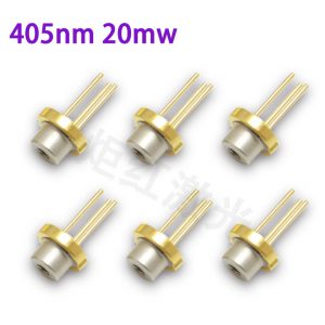 φ5.6mm SLD3132VF Blue-violet UV 405nm 20mW Laser Diode for Laser Modules
Reviews
There are no reviews yet.