
 electron beams")
Description
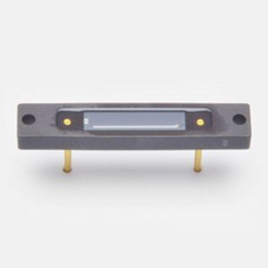
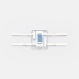
Hamamatsu S11142-10 High sensitivity, direct detection of low energy (1 keV or more) electron beams
Features
– Direct detection of low energy (1 keV or more) electron beams with high sensitivity
– High gain: 300 times
high detection efficiency: 72 % (incident electronenergy: 1.5 keV)
– Large photosensitive area size: 14 × 14 mm
– φ2.0 mm hole in center of photosensitive area
– 4-element photodiode
– Thin ceramic package
– Uses a wiring board made of less magnetic materials
Notice
The chip of this product is not sealed and is exposed.
Parts such as electrodes on the chip are not protected by an enclosure or window and so require especially strict care during handling compared to ordinary products.
Specifications
| Photosensitive area | 14 × 14 mm |
|---|---|
| Number of elements | 4 |
| Package | Ceramic |
| Package category | Unsealed |
| Incident electron energy range (typ.) | 1 to 30 keV |
| Electron multiplying gain (typ.) | 300 |
| Reverse voltage (max.) | 20 V |
| Dark current (max.) | 60000 pA |
| Cutoff frequency (typ.) | 5 MHz |
| Terminal capacitance (typ.) | 200 pF |
| Measurement condition | Ta=25 ℃, VR=5 V |


Reviews
There are no reviews yet.