

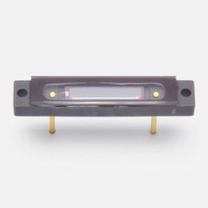
Description
The S13620-02 is an 8 × 8 element Si photodiode array with a back-illuminated type structure for X-ray non-destructive inspection. The back-illuminated photodiode array is easy to handle because there are no bonding wires or photosensitive area on the incident surface side. You can mount a scintillator without being concerned about damaging wires. In addition, it is designed with minimal dead space around the product. This makes it possible to arrange multiple products side by side. There is no crosstalk between channels.
Features
-2D (8 × 8 element) array
-Spectral response range: 400 to 1100 nm
-Package size: 24 (W) × 24 (H) mm
-Element pitch: 3.0 mm × 64 elements
-Easy coupling with a scintillator
Because there are no wires in the photosensitive area and the optical coupling effi ciency with an scintillator can be maximized, it suitable for non-destructive X-ray inspection equipment.
Notice
The chip of this product is not sealed and is exposed.
Parts such as electrodes on the chip are not protected by an enclosure or window and so require especially strict care during handling compared to ordinary products.
Specifications
| Element size (per 1 element) | 2.5 × 2.5 mm |
|---|---|
| Number of elements | 64 |
| Package | Glass epoxy |
| Package category | Unsealed |
| Scintillator type | None |
| Cooling | Non-cooled |
| Reverse voltage (max.) | 10 V |
| Spectral response range | 400 to 1100 nm |
| Peak sensitivity wavelength (typ.) | 960 nm |
| Photosensitivity (typ.) | 0.61 A/W |
| Dark current (max.) | 300 pA |
| Rise time (typ.) | 15 μs |
| Terminal capacitance (typ.) | 60 pF |
| Note | These products are also available as scintillator-mounted products (custom order products) such as CsI (Tl), phosphor sheet, GOS, and CWO. Consult with your nearest Hamamatsu sales office. |
| Measurement condition | Ta=25 ℃, per element, Photosensitivity: λ=920 nm |


Reviews
There are no reviews yet.