

Description
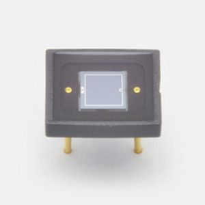
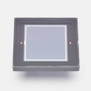
Hamamatsu S13955-01 Back-illuminated photodiodes with CSP structure
A scintillator can be coupled directly on the chip by using a back-illuminated photodiode. It is designed with minimal dead space around the product. This makes it possible to arrange multiple products side by side.
Features
– Spectral response range: 400 to 1100 nm
– Package size: 7.52 × 7.52 mm
– Easy coupling to scintillator
– Easy coupling with a scintillator
Because there are no wires in the photosensitive area and the optical coupling efficiency with an scintillator can be maximized, it suitable for non-destructive X-ray inspection equipment.
Notice
The chip of this product is not sealed and is exposed.
Parts such as electrodes on the chip are not protected by an enclosure or window and so require especially strict care during handling compared to ordinary products.
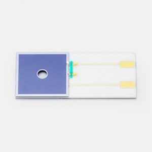
Specifications
| Photosensitive area | 6.97 × 6.97 mm |
|---|---|
| Package | Glass epoxy |
| Package category | Unsealed |
| Cooling | Non-cooled |
| Reverse voltage (max.) | 10 V |
| Spectral response range | 400 to 1100 nm |
| Peak sensitivity wavelength (typ.) | 960 nm |
| Photosensitivity (typ.) | 0.61 A/W |
| Dark current (max.) | 1000 pA |
| Rise time (typ.) | 15 μs |
| Terminal capacitance (typ.) | 500 pF |
| Measurement condition | Typ. Ta=25 ℃, Photosensitivity: λ=920 nm, Dark current: VR=10 mV, Terminal capacitance: VR=0 V, f=10 kH, unless otherwise noted |


Reviews
There are no reviews yet.