Specifications of HER504 diode
Maximum Recurrent Peak Reverse Voltage: 300 V
Maximum Average Forward Output Current: 5 A
Maximum Forward Voltage Drop per element at 1.0A DC: 1.3 V
Maximum reverse recovery time: 75 ns
Typical Junction Capacitance: 70 pF
Package: DO-27
Weight: 0.4 grams
Operating and Storage Temperature Range: -65…+150 °C
The HER504 diode has a cathode (-) and anode (+). In the schematic symbol, the tip of the triangle with the line on top of it is the cathode. The cathode is marked on the body of a diode by a band as shown below.
The current can flow from only the anode to the cathode and never from the cathode to the anode – the HER504 diode is like a one way electric valve.
Diode: rectifying; THT; 300V; 5A; Ammo Pack; Ifsm: 150A; DO27; 75ns
Manufacturer DC COMPONENTS
Type of diode rectifying
Mounting THT
Max. off-state voltage 300V
Load current 5A
Semiconductor structure single diode
Features of semiconductor devices fast switching
Kind of package Ammo Pack
Max. forward impulse current 150A
Case DO27
Max. forward voltage 1.3V
Reverse recovery time 75ns
High current capability High surge current capability High reliability Low reverse current Low forward voltage drop Fast switching for high efficiency
- Case : DO-201AD Molded plastic * Epoxy : UL94V-O rate flame retardant * Lead : Axial lead solderable per MIL-STD-202, Method 208 guaranteed * Polarity : Color band denotes cathode end * Mounting position : Any * Weight : 1.16 grams
Rating 25 °C ambient temperature unless otherwise specified. Single phase, half wave, 60 Hz, resistive or inductive load. For capacitive load, derate current by 20%.
Maximum Recurrent Peak Reverse Voltage Maximum RMS Voltage Maximum DC Blocking Voltage Maximum Average Forward Current 0.375″(9.5mm) Lead Length 55 °C Maximum Peak Forward Surge Current, 8.3ms Single half sine wave superimposed on rated load (JEDEC Method) Maximum Forward Voltage 5.0 A Maximum DC Reverse Current at Rated DC Blocking Voltage 100 °C
Maximum Reverse Recovery Time ( Note 1 ) Typical Junction Capacitance ( Note 2 ) Junction Temperature Range Storage Temperature Range
1 ) Reverse Recovery Test Conditions 1.0 A, Irr 2 ) Measured at 1.0 MHz and applied reverse voltage of 4.0 VDC
FIG.1 – REVERSE RECOVERY TIME CHARACTERISTIC AND TEST CIRCUIT DIAGRAM
NOTES : 1. Rise Time 7 ns max., Input Impedance = 1 megaohm, 22 pF. 2. Rise time 10 ns max., Source Impedance = 50 ohms. 3. All Resistors = Non-inductive Types.
FIG.3 – MAXIMUM NON-REPETITIVE PEAK FORWARD SURGE CURRENT PEAK FORWARD SURGE CURRENT, AMPERES
AMBIENT TEMPERATURE, ( °C) FIG.4 – TYPICAL FORWARD CHARACTERISTICS REVERSE CURRENT, MICROAMPERES


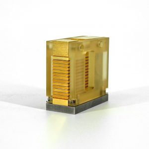
 Alma Soprano 808nm Diode Laser bar stack