The PN junction diode is made up of two regions: p and n, separated by a depletion region where charge is stored. The effect described in the previous tutorial is achieved without applying any external voltage to the actual PN junction, resulting in the junction being in an equilibrium state.
However, by making electrical connections at the ends of both the N-type and P-type materials and connecting them to a battery source, we now have an additional energy source to overcome the potential barrier.
The addition of this additional energy source causes free electrons to be able to cross the depletion region from one side to the other. The PN junction’s behavior in relation to the potential barrier’s width results in an asymmetrical conducting two terminal device known as the PN Junction Diode.
A PN Intersection A diode is one of the most basic semiconductor devices, with the electrical property of passing current through itself in only one direction. A diode, unlike a resistor, does not behave linearly in relation to the applied voltage. Because it has an exponential current-voltage (I-V) relationship, we cannot simply describe its operation with an equation like Ohm’s law.
A suitable positive voltage (forward bias) applied between the two ends of the PN junction can provide free electrons and holes with the extra energy needed to cross the junction as the width of the depletion layer around the PN junction decreases.
Applying a negative voltage (reverse bias) causes the free charges to be pulled away from the junction, increasing the depletion layer width. This increases or decreases the effective resistance of the junction, allowing or blocking current flow through the diode’s pn-junction.
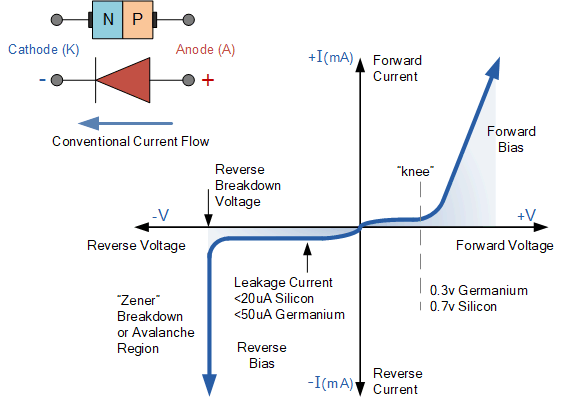
The depletion layer then widens with increasing reverse voltage application and narrows with increasing forward voltage application. This is due to differences in the electrical properties of the two sides of the PN junction, which cause physical changes. One of the outcomes is rectification, as seen in the static I-V (current-voltage) characteristics of PN junction diodes. Rectification is demonstrated by an asymmetrical current flow when the bias voltage polarity is changed, as shown below.
